Global Semiconductor Lithography Equipment Market Size, Trends, and Analysis - Forecasts To 2026 By Technology (KrF, i-line, ArF Dry, EUV, and ArF Immersion), By Industry (Government, Retail & Consumer Goods, Telecommunication, Manufacturing, BFSI, and Others), By End-User (IDM, Foundry, and Memory), By Region (North America, Asia Pacific, CSA, Europe, and the Middle East and Africa); End-User Landscape, Company Market Share Analysis & Competitor Analysis
Globally, the use of semiconductor photolithography equipment is becoming more mainstream. During the past few years, the pervasive use of semiconductor lithography devices for the technological development of tablets, smartphones, and computers has increased significantly. The demand for semiconductor lithography is driven by the increased demand for smarter and better consumer electronics. Also, semiconductor lithography systems are used to manufacture ICs that are installed in various applications, such as electronic communication devices, consumer devices, sensor devices, and memory devices. The growth in the use of ICs has also had a positive effect on the development of the demand for semiconductor lithography equipment.
Besides, the requirement for large panel displays and portable electronic devices to be installed has led to stimulating the need for KrF and ArF lithography systems, which is anticipated to propel the market demand for semiconductor lithography equipment during the forecast period. Despite the different advantages provided by semiconductor photolithography equipment, there are, however, certain limiting factors that hinder market development. Uncertain economic conditions in diverse regions are the biggest impeding factor behind the development of this market.
![]()
Based on the technology, the market is categorized as KrF, i-line, ArF Dry, EUV, and ArF Immersion. Extreme Ultraviolet Lithography (EUV) is foreseen to dominate the market. Over the years, semiconductor lithography machines have made numerous advancements, introducing a large lens with a high numeral aperture (NA) or using light as the light source for short wavelengths. However, as the length of the gate reduces below 30nm, the patterning ability of current ArF lithography equipment for liquid immersion approaches its threshold.
The semiconductor industry has therefore been planning new semiconductor lithography under the name EUV in order to facilitate 10nm-class scale processing. EUV enables much better semiconductor circuit patterns without multi-patterning by using the light of a 13.5nm wavelength, much smaller than the current 193nm ArF wavelength. This decreases the number of manufacturing steps and hence shortens the output time of current multi-patterning, such as the Quadruple Patterning Technique. Applying EUV to chips like DRAMs, however, is a demanding method that needs the most sophisticated technologies. With respect to DRAMs, EUV is expected to be partly used in the manufacture of chips of 1ynm or less.
Based on the industry, the market has been segmented into manufacturing, retail & consumer goods, BFSI, telecommunication, government, and others. The manufacturing sector is likely to hold the largest market share of semiconductor lithography equipment.
The development in the manufacturing sector is attributed to the increase in demand for portable electronic products that use lithography techniques for manufacturing ICs, such as smart homes and fitness trackers, smartphones, and tablets. In addition, increasing investments by manufacturers in research & development activities to introduce technological innovations and deliver low-cost, high-precision semiconductor tools will stimulate the demand for lithography equipment in the near future.
According to the end-user, the market is categorized as IDM, foundry, and memory. IDM is foreseen to hold the largest market share due to increased investment by IDM companies to improve their R&D efforts for technically advanced and miniaturized products, like ultra-low-power microcontrollers, smart ICs, sensors, and RFID circuits, to fulfill strong demand in different verticals of the market.
IDM businesses also focus investments in upgrading their manufacturing facilities for specialized semiconductor devices, boosting demand for semiconductor manufacturing facilities. In April 2019, Texas Instruments declared that USD 3.1 billion will be spent on the construction of a new 300-millimeter wafer production facility in Texas, U.S. This new market growth would allow the company to increase the production of chips for a broad variety of applications, namely connected cars, industrial machinery, and smartphones.
![]()
Due to the rise in the semiconductor industry combined with the involvement of a huge number of equipment manufacturers, the Asia Pacific lithography equipment market is likely to lead the global semiconductor lithography equipment market. Growing government financial assistance is attracting businesses to invest in the development of semiconductor manufacturing plants in the country. The Government of India is funding the development of a manufacturing facility using the new Gallium Nitride technology (semiconductor fab of GaN). Likewise, the Government of China revealed in May 2018 that it will spend approximately USD 50 billion to boost its ability to produce and develop semiconductor chips. Such high government adoption of portable electronic devices and programs is expected to contribute to the development of the semiconductor lithography equipment market in the country. Taiwan, South Korea, and Japan are the primary contributors to the market's growth in the Asia Pacific. The presence of numerous renowned semiconductor foundries in the region is driving up demand for photolithography equipment. The presence of significant companies in the region's mobile devices and consumer electronics markets supports the demand for semiconductor products.
The North American market is expected to develop moderately. Deployment of semiconductor lithography equipment would be accelerated by the incorporation of sophisticated technologies in semiconductor production equipment, such as AI and IoT. As a result, the semiconductor manufacturing equipment market participants are likely to benefit from attractive growth prospects. Moreover, as IoT device proliferation develops as a consequence of the covid-19 pandemic, the development of chip industries in developing countries, and the increase in the volume of data centers and servers are all variables that would enhance the sales in the semiconductor lithography equipment market.
ASML Holding, SÜSS MICROTEC SE., Tokyo Electron Limited, Nikon Corporation, Applied Materials, Inc., EOL IT Services, Canon Inc., NuFlare Technology Inc., JEOL, Ltd., and Vistec Semiconductor Systems are the key vendors competing in the semiconductor lithography equipment market.
Please note: This is not an exhaustive list of companies profiled in the report.
Chapter 1 Methodology
1.1 Market Scope & Definitions
1.2 Estimates & Forecast Calculation
1.3 Historical Data Overview And Validation
1.4 Data Types
1.4.1 Secondary
1.4.2 Primary
Chapter 2 Report Outlook
2.1 Global Semiconductor Lithography Equipment Industry Overview, 2016-2026
2.1.1 Industry Overview
2.1.2 Technology Overview
2.1.3 Industry Overview
2.1.4 End-User Overview
2.1.5 Regional Overview
Chapter 3 Global Semiconductor Lithography Equipment Market Trends
3.1 Market Segmentation
3.2 Industry Background, 2016-2026
3.3 Market Key Trends
3.3.1 Positive Trends
3.3.1.1 Growing Trends of Miniaturization of Semiconductor Components
3.3.1.2 Increasing Number of Fabless Semiconductor Companies
3.3.2 Industry Challenges
3.3.2.1 Uncertain Economic Conditions
3.4 Prospective Growth Scenario
3.4.1 Technology Growth Scenario
3.4.2 Industry Growth Scenario
3.4.3 End-User Growth Scenario
3.5 COVID-19 Influence over Industry Growth
3.6 Porter’s Analysis
3.7 PESTEL Analysis
3.8 Value Chain & Supply Chain Analysis
3.9 Regulatory Framework
3.9.1 North America
3.9.2 Europe
3.9.3 APAC
3.9.4 LATAM
3.9.5 MEA
3.10 Technology Overview
3.11 Market Share Analysis, 2020
3.11.1 Company Positioning Overview, 2020
Chapter 4 Global Semiconductor Lithography Equipment Market, By Technology
4.1 Technology Outlook
4.2 KrF
4.2.1 Market Size, By Region, 2016-2026 (USD Million)
4.3 i-line
4.3.1 Market Size, By Region, 2016-2026 (USD Million)
4.4 ArF Dry
4.4.1 Market Size, By Region, 2016-2026 (USD Million)
4.5 EUV
4.5.1 Market Size, By Region, 2016-2026 (USD Million)
4.6 ArF Immersion
4.6.1 Market Size, By Region, 2016-2026 (USD Million)
Chapter 5 Global Semiconductor Lithography Equipment Market, By Industry
5.1 Industry Outlook
5.2 Government
5.2.1 Market Size, By Region, 2016-2026 (USD Million)
5.3 Retail & Consumer Goods
5.3.1 Market Size, By Region, 2016-2026 (USD Million)
5.4 Telecommunication
5.4.1 Market Size, By Region, 2016-2026 (USD Million)
5.5 Manufacturing
5.5.1 Market Size, By Region, 2016-2026 (USD Million)
5.6 BFSI
5.6.1 Market Size, By Region, 2016-2026 (USD Million)
5.7 Others
5.7.1 Market Size, By Region, 2016-2026 (USD Million)
Chapter 6 Global Semiconductor Lithography Equipment Market, By End-User
6.1 End-User Outlook
6.2 IDM
6.2.1 Market Size, By Region, 2016-2026 (USD Million)
6.3 Foundry
6.3.1 Market Size, By Region, 2016-2026 (USD Million)
6.4 Memory
6.4.1 Market Size, By Region, 2016-2026 (USD Million)
Chapter 7 Global Semiconductor Lithography Equipment Market, By Region
7.1 Regional outlook
7.2 North America
7.2.1 Market Size, By Country, 2016-2026 (USD Million)
7.2.2 Market Size, By Technology, 2016-2026 (USD Million)
7.2.3 Market Size, By Industry, 2016-2026 (USD Million)
7.2.4 Market Size, By End-User, 2016-2026 (USD Million)
7.2.5 U.S.
7.2.5.1 Market Size, By Technology, 2016-2026 (USD Million)
7.2.5.2 Market Size, By Industry, 2016-2026 (USD Million)
7.2.5.3 Market Size, By End-User, 2016-2026 (USD Million)
7.2.6 Canada
7.2.6.1 Market Size, By Technology, 2016-2026 (USD Million)
7.2.6.2 Market Size, By Industry, 2016-2026 (USD Million)
7.2.6.3 Market Size, By End-User, 2016-2026 (USD Million)
7.3 Europe
7.3.1 Market Size, By Country, 2016-2026 (USD Million)
7.3.2 Market Size, By Technology, 2016-2026 (USD Million)
7.3.3 Market Size, By Industry, 2016-2026 (USD Million)
7.3.4 Market Size, By End-User, 2016-2026 (USD Million)
7.3.5 Germany
7.3.5.1 Market Size, By Technology, 2016-2026 (USD Million)
7.3.5.2 Market Size, By Industry, 2016-2026 (USD Million)
7.3.5.3 Market Size, By End-User, 2016-2026 (USD Million)
7.3.6 UK
7.3.6.1 Market Size, By Technology, 2016-2026 (USD Million)
7.3.6.2 Market Size, By Industry, 2016-2026 (USD Million)
7.3.6.3 Market Size, By End-User, 2016-2026 (USD Million)
7.3.7 France
7.3.7.1 Market Size, By Technology, 2016-2026 (USD Million)
7.3.7.2 Market Size, By Industry, 2016-2026 (USD Million)
7.3.7.3 Market Size, By End-User, 2016-2026 (USD Million)
7.3.8 Italy
7.3.8.1 Market Size, By Technology, 2016-2026 (USD Million)
7.3.8.2 Market Size, By Industry, 2016-2026 (USD Million)
7.3.8.3 Market Size, By End-User, 2016-2026 (USD Million)
7.3.9 Spain
7.3.9.1 Market Size, By Technology, 2016-2026 (USD Million)
7.3.9.2 Market Size, By Industry, 2016-2026 (USD Million)
7.3.9.3 Market Size, By End-User, 2016-2026 (USD Million)
7.3.10 Russia
7.3.10.1 Market Size, By Technology, 2016-2026 (USD Million)
7.3.10.2 Market Size, By Industry, 2016-2026 (USD Million)
7.3.10.3 Market Size, By End-User, 2016-2026 (USD Million)
7.4 Asia Pacific
7.4.1 Market Size, By Country, 2016-2026 (USD Million)
7.4.2 Market Size, By Technology, 2016-2026 (USD Million)
7.4.3 Market Size, By Industry, 2016-2026 (USD Million)
7.4.4 Market Size, By End-User, 2016-2026 (USD Million)
7.4.5 China
7.4.5.1 Market Size, By Technology, 2016-2026 (USD Million)
7.4.5.2 Market Size, By Industry, 2016-2026 (USD Million)
7.4.5.3 Market Size, By End-User, 2016-2026 (USD Million)
7.4.6 India
7.4.6.1 Market Size, By Technology, 2016-2026 (USD Million)
7.4.6.2 Market Size, By Industry, 2016-2026 (USD Million)
7.4.6.3 Market Size, By End-User, 2016-2026 (USD Million)
7.4.7 Japan
7.4.7.1 Market Size, By Technology, 2016-2026 (USD Million)
7.4.7.2 Market Size, By Industry, 2016-2026 (USD Million)
7.4.7.3 Market Size, By End-User, 2016-2026 (USD Million)
7.4.8 Australia
7.4.8.1 Market Size, By Technology, 2016-2026 (USD Million)
7.4.8.2 Market size, By Industry, 2016-2026 (USD Million)
7.4.8.3 Market Size, By End-User, 2016-2026 (USD Million)
7.4.9 South Korea
7.4.9.1 Market Size, By Technology, 2016-2026 (USD Million)
7.4.9.2 Market Size, By Industry, 2016-2026 (USD Million)
7.4.9.3 Market Size, By End-User, 2016-2026 (USD Million)
7.5 Latin America
7.5.1 Market Size, By Country, 2016-2026 (USD Million)
7.5.2 Market Size, By Technology, 2016-2026 (USD Million)
7.5.3 Market Size, By Industry, 2016-2026 (USD Million)
7.5.4 Market Size, By End-User, 2016-2026 (USD Million)
7.5.5 Brazil
7.5.5.1 Market Size, By Technology, 2016-2026 (USD Million)
7.5.5.2 Market Size, By Industry, 2016-2026 (USD Million)
7.5.5.3 Market Size, By End-User, 2016-2026 (USD Million)
7.5.6 Mexico
7.5.6.1 Market Size, By Technology, 2016-2026 (USD Million)
7.5.6.2 Market Size, By Industry, 2016-2026 (USD Million)
7.5.6.3 Market Size, By End-User, 2016-2026 (USD Million)
7.5.7 Argentina
7.5.7.1 Market Size, By Technology, 2016-2026 (USD Million)
7.5.7.2 Market Size, By Industry, 2016-2026 (USD Million)
7.5.7.3 Market Size, By End-User, 2016-2026 (USD Million)
7.6 MEA
7.6.1 Market Size, By Country, 2016-2026 (USD Million)
7.6.2 Market Size, By Technology, 2016-2026 (USD Million)
7.6.3 Market Size, By Industry, 2016-2026 (USD Million)
7.6.4 Market Size, By End-User, 2016-2026 (USD Million)
7.6.5 Saudi Arabia
7.6.5.1 Market Size, By Technology, 2016-2026 (USD Million)
7.6.5.2 Market Size, By Industry, 2016-2026 (USD Million)
7.6.5.3 Market Size, By End-User, 2016-2026 (USD Million)
7.6.6 UAE
7.6.6.1 Market Size, By Technology, 2016-2026 (USD Million)
7.6.6.2 Market Size, By Industry, 2016-2026 (USD Million)
7.6.6.3 Market Size, By End-User, 2016-2026 (USD Million)
7.6.7 South Africa
7.6.7.1 Market Size, By Technology, 2016-2026 (USD Million)
7.6.7.2 Market Size, By Industry, 2016-2026 (USD Million)
7.6.7.3 Market Size, By End-User, 2016-2026 (USD Million)
Chapter 8 Company Landscape
8.1 Competitive Analysis, 2020
8.2 ASML Holding
8.2.1 Company Overview
8.2.2 Financial Analysis
8.2.3 Strategic Positioning
8.2.4 Info Graphic Analysis
8.3 SÜSS MICROTEC SE.
8.3.1 Company Overview
8.3.2 Financial Analysis
8.3.3 Strategic Positioning
8.3.4 Info Graphic Analysis
8.4 Tokyo Electron Limited
8.4.1 Company Overview
8.4.2 Financial Analysis
8.4.3 Strategic Positioning
8.4.4 Info Graphic Analysis
8.5 Nikon Corporation
8.5.1 Company Overview
8.5.2 Financial Analysis
8.5.3 Strategic Positioning
8.5.4 Info Graphic Analysis
8.6 Applied Materials, Inc.
8.6.1 Company Overview
8.6.2 Financial Analysis
8.6.3 Strategic Positioning
8.6.4 Info Graphic Analysis
8.7 EOL IT Services, Canon Inc.
8.7.1 Company Overview
8.7.2 Financial Analysis
8.7.3 Strategic Positioning
8.7.4 Info Graphic Analysis
8.8 NuFlare Technology Inc.
8.8.1 Company Overview
8.8.2 Financial Analysis
8.8.3 Strategic Positioning
8.8.4 Info Graphic Analysis
8.9 Mylan Laboratories Limited
8.9.1 Company Overview
8.9.2 Financial Analysis
8.9.3 Strategic Positioning
8.9.4 Info Graphic Analysis
8.10 JEOL, Ltd.
8.10.1 Company Overview
8.10.2 Financial Analysis
8.10.3 Strategic Positioning
8.10.4 Info Graphic Analysis
8.11 Vistec Semiconductor Systems
8.11.1 Company Overview
8.11.2 Financial Analysis
8.11.3 Strategic Positioning
8.11.4 Info Graphic Analysis
8.12 Other Companies
8.12.1 Company Overview
8.12.2 Financial Analysis
8.12.3 Strategic Positioning
8.12.4 Info Graphic Analysis
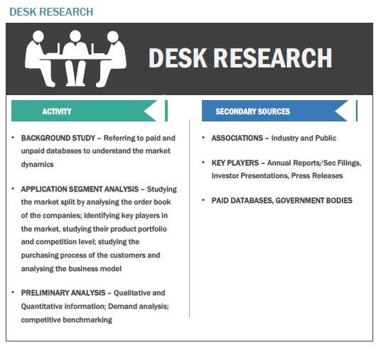
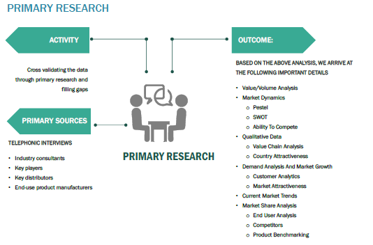
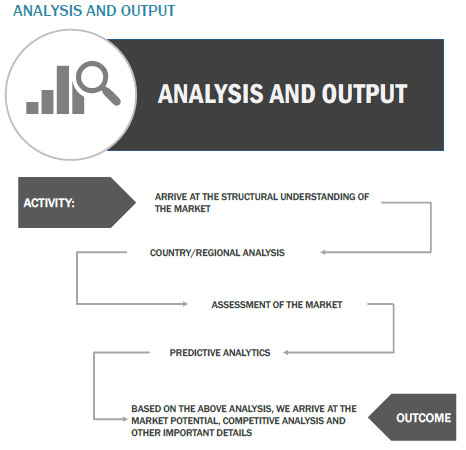
The Global Semiconductor Lithography Equipment Market has been studied from the year 2019 till 2026. However, the CAGR provided in the report is from the year 2021 to 2026. The research methodology involved three stages: Desk research, Primary research, and Analysis & Output from the entire research process.

The desk research involved a robust background study which meant referring to paid and unpaid databases to understand the market dynamics; mapping contracts from press releases; identifying the key players in the market, studying their product portfolio, competition level, annual reports/SEC filings & investor presentations; and learning the demand and supply-side analysis for the Semiconductor Lithography Equipment Market.

The primary research activity included telephonic conversations with more than 50 tier 1 industry consultants, distributors, and end-use product manufacturers.

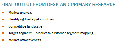
Finally, based on the above thorough research process, an in-depth analysis was carried out considering the following aspects: market attractiveness, current & future market trends, market share analysis, SWOT analysis of the company and customer analytics.

Frequently Asked Questions
Tailor made solutions just for you
80% of our clients seek made-to-order reports. How do you want us to tailor yours?
OUR CLIENTS